School of Electronic & Information Engineering
Nanjing University of Information Science & Technology (NUIST)
China
Homepage
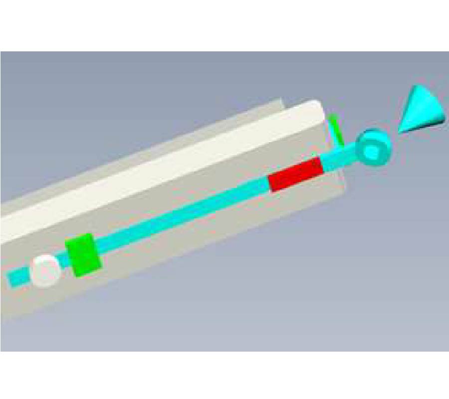
![]()
![]()
![]()
1. Deutsch, A., G. V. Kopcsay, P. Restle, G. Katopis, W. D. Becker, H. Smith, P. W. Coteus, C. W. Surovic, B. J. Rubin, R. P. Dunne, T. Gallo, K. A. Jenkins, L. M. Terman, R. H. Dennard, G. A. Sai-Halasz, and D. R. Knebel, "When are transmission-line effects important for on-chip interconnections?," IEEE Trans. Microwave Theory and Techniques, Vol. 45, 1836-1846, Oct. 1997.
doi:10.1109/22.641781 Google Scholar
2. Eudes, T., B. Ravelo, T. Lacrevaz, and B. Flechet, "Distributed model of two-level asymmetrical PCB interconnect tree," Proc. of 2013 International Symposium on Electromagnetic Compatibility (EMC Europe), 132-137, Brugge, Belgium, Sep. 2-6, 2013. Google Scholar
3. Ravelo, B., "Delay modelling of high-speed distributed interconnect for the signal integrity prediction," Eur. Phys. J. Appl. Phys., Vol. 57, 31002-1-31002-8, Feb. 2012. Google Scholar
4. Buckwalter, J. F., "Predicting microwave digital signal integrity," IEEE Trans. Advanced Packaging, Vol. 32, No. 2, 280-289, May 2009.
doi:10.1109/TADVP.2008.2011560 Google Scholar
5. Zhang, G.-H., M. Xia, and X.-M. Jiang, "Transient analysis of wire structures using time domain integral equation method with exact matrix elements," Progress In Electromagnetics Research, Vol. 92, 281-298, 2009.
doi:10.2528/PIER09032003 Google Scholar
6. Ravelo, B., "Behavioral model of symmetrical multi-level T-tree interconnects," Progress In Electromagnetics Research B, Vol. 41, 23-50, 2012.
doi:10.2528/PIERB12040205 Google Scholar
7. Muller, E. W., J. A. Panitz, and S. B. McLane, "The atom probe field ion microscope," Review of Scientific Instruments, Vol. 39, No. 1, 83-88, 1968.
doi:10.1063/1.1683116 Google Scholar
8. Blavette, D., A. Bostel, J. M. Sarrau, B. Deconihout, and A. Menand, "An atom-probe for three dimensional tomography," Nature, Vol. 363, 432-435, 1993.
doi:10.1038/363432a0 Google Scholar
9. Gault, B., F. Vurpillot, A. Vella, M. Gilbert, A. Menand, D. Blavette, and B. Deconihout, "Design of a femtosecond laser assisted tomographic atom probe," Review of Scientific Instruments, Vol. 77, No. 4, 043705, 2006.
doi:10.1063/1.2194089 Google Scholar
10. Kelly, T. F. and M. K. Miller, "Atom probe tomography," Review of Scientific Instruments, Vol. 78, No. 3, 031101, 2007.
doi:10.1063/1.2709758 Google Scholar
11. Menand, A. and D. Blavette, "Sonde atomique tridimensionnelle,", P902, 1-7, Techniques de l'Ingenieur, Jul. 1995 (in French). Google Scholar
12. Vurpillot, F. and A. Bostel, "Tomographic atomic probe comprising a high voltage electric pulse electro-optical generator,", Patent No. 057721, 2010. Google Scholar
13. Gault, B., M. P. Moody, J. M. Cairney, and S. P. Ringer, "Atom probe microscopy," Springer Series in Materials Science, Vol. 160, 29-68, 2012.
doi:10.1007/978-1-4614-3436-8_3 Google Scholar
14. Kelly, T. F., T. T. Gribb, J. D. Olson, R. L. Martens, J. D. Shepard, S. A. Wiener, T. C. Kunicki, R. M. Ulfg, D. R. Lenz, E. M. Strennen, E. Oltman, J. H. Bunton, and D. R. Strait, "First data from a commercial local electrode atom probe (LEAP)," Microscopy and Microanalysis, Vol. 10, 373-383, 2004.
doi:10.1017/S1431927604040565 Google Scholar
15. Miller, M. K., "Atom probe tomography and field ion microscopy: Ion-beam techniques," Characterization of Materials, 2nd Edition, May 2012, Doi: 10.1002/0471266965.com145. Google Scholar
16. Tourek, C. J., "Application of atom probe tomography to the investigation of atomic force microscope tips and interfacial phenomena,", Ph.D. Thesis, Iowa State University, USA, 2012. Google Scholar
18., www.belke.com. Google Scholar
18. Kohler, S., V. Couderc, R. P. O'connor, D. Arnaud-Cormos, and P. Leveque, "A versatile high voltage nano- and sub-nanosecond pulse generator," IEEE Trans. Dielectrics and Electrical Insulation, Vol. 20, No. 4, 1201-1208, Aug. 2013.
doi:10.1109/TDEI.2013.6571435 Google Scholar
19. Yuan, J., Yuan, J., W. Xie, H. Liu, J. Liu, H. Li, X. Wang, and W. Jiang, "High-power semi-insulating GaAs photoconductive semiconductor switch employing extrinsic photoconductivity," IEEE Trans. Plasma Sci., Vol. 37, No. 10, 1959-1963, Oct. 2009.
doi:10.1109/TPS.2009.2022013 Google Scholar
20. European Standard "Connector for electronic equipment --- Tests measurements --- Part 25-7: Test 25g --- Impedance, reflection coe±cient and voltage standing wave ratio (VSWR),", NF EN 60512-25-7, Jun. 2005. Google Scholar
21. Blood Jr., W. R., ECL System Design Handbook, 45 & 48, Motorola Semiconductor Products, Inc., Phoenix, AZ , 1988.
22. Buchanan, J. E., BiCMOS/CMOS Systems Design, 109, McGraw-Hill, New York, 1991.