Vol. 110
Latest Volume
All Volumes
PIERL 119 [2024] PIERL 118 [2024] PIERL 117 [2024] PIERL 116 [2024] PIERL 115 [2024] PIERL 114 [2023] PIERL 113 [2023] PIERL 112 [2023] PIERL 111 [2023] PIERL 110 [2023] PIERL 109 [2023] PIERL 108 [2023] PIERL 107 [2022] PIERL 106 [2022] PIERL 105 [2022] PIERL 104 [2022] PIERL 103 [2022] PIERL 102 [2022] PIERL 101 [2021] PIERL 100 [2021] PIERL 99 [2021] PIERL 98 [2021] PIERL 97 [2021] PIERL 96 [2021] PIERL 95 [2021] PIERL 94 [2020] PIERL 93 [2020] PIERL 92 [2020] PIERL 91 [2020] PIERL 90 [2020] PIERL 89 [2020] PIERL 88 [2020] PIERL 87 [2019] PIERL 86 [2019] PIERL 85 [2019] PIERL 84 [2019] PIERL 83 [2019] PIERL 82 [2019] PIERL 81 [2019] PIERL 80 [2018] PIERL 79 [2018] PIERL 78 [2018] PIERL 77 [2018] PIERL 76 [2018] PIERL 75 [2018] PIERL 74 [2018] PIERL 73 [2018] PIERL 72 [2018] PIERL 71 [2017] PIERL 70 [2017] PIERL 69 [2017] PIERL 68 [2017] PIERL 67 [2017] PIERL 66 [2017] PIERL 65 [2017] PIERL 64 [2016] PIERL 63 [2016] PIERL 62 [2016] PIERL 61 [2016] PIERL 60 [2016] PIERL 59 [2016] PIERL 58 [2016] PIERL 57 [2015] PIERL 56 [2015] PIERL 55 [2015] PIERL 54 [2015] PIERL 53 [2015] PIERL 52 [2015] PIERL 51 [2015] PIERL 50 [2014] PIERL 49 [2014] PIERL 48 [2014] PIERL 47 [2014] PIERL 46 [2014] PIERL 45 [2014] PIERL 44 [2014] PIERL 43 [2013] PIERL 42 [2013] PIERL 41 [2013] PIERL 40 [2013] PIERL 39 [2013] PIERL 38 [2013] PIERL 37 [2013] PIERL 36 [2013] PIERL 35 [2012] PIERL 34 [2012] PIERL 33 [2012] PIERL 32 [2012] PIERL 31 [2012] PIERL 30 [2012] PIERL 29 [2012] PIERL 28 [2012] PIERL 27 [2011] PIERL 26 [2011] PIERL 25 [2011] PIERL 24 [2011] PIERL 23 [2011] PIERL 22 [2011] PIERL 21 [2011] PIERL 20 [2011] PIERL 19 [2010] PIERL 18 [2010] PIERL 17 [2010] PIERL 16 [2010] PIERL 15 [2010] PIERL 14 [2010] PIERL 13 [2010] PIERL 12 [2009] PIERL 11 [2009] PIERL 10 [2009] PIERL 9 [2009] PIERL 8 [2009] PIERL 7 [2009] PIERL 6 [2009] PIERL 5 [2008] PIERL 4 [2008] PIERL 3 [2008] PIERL 2 [2008] PIERL 1 [2008]
2023-06-13
PIER Letters
Vol. 110, 127-135, 2023
download: 113
A Loaded Line 2-Bit Phase Shifter Using RF MEMS DC/Capacitive Switches
Niharika Narang , Pranav K. Shrivastava , Ananjan Basu and Pushpapraj Singh
This letter presents the fabrication and measurement of a novel loaded line phase shifter design providing four different phase shifts using only two RF MEMS switches. The flexibility of choosing DC or capacitive load depending upon the phase shift required in a single RF MEMS switch makes the phase shifter compact and requires less no. of proposed switches. The RF MEMS Switch has been designed to provide isolation better than 10 dB in both DC and capacitive states from 16 to 45 GHz. Due to the designed RF MEMS beam switching between DC and capacitive loading, the proposed phase shifter provides a 2-bit phase shift using only two switches. The measured phase shifter has the maximum insertion loss of 0.8 dB with a bandwidth of 8 GHz from 16 to 24 GHz. The return loss is better than 10 dB for all four states. The maximum Root-Mean-Square (RMS) insertion loss error is 0.28 dB, and the phase shift error is 0.98º. The proposed phase shifter is fabricated using the surface micromachining on the sapphire substrate and occupies an area of 3.931 mm2.
A Loaded Line 2-bit Phase Shifter Using RF MEMS DC/Capacitive Switches
2023-06-02
PIER Letters
Vol. 110, 117-126, 2023
download: 134
MIMO Antenna with Reduced Mutual Coupling Using Circular Ring Neutralization Structure
Kondapalli Venu Gopal and Yarravarapu Srinivasa Rao
In this article, a 15 × 20 mm2 arbitrary-shaped antenna is built. The same is extended to a 2 × 2 MIMO antenna with size 32 × 20 mm2. It covers two bands. Band-1 covers 3-4.44 GHz, and band-2 covers 5.32-11.1 GHz. In this case, a circular neutralization structure is used to lessen the mutual coupling between the two ports. The ECC, DG, CCL, and radiation pattern are used to demonstrate how well the MIMO antenna performs. Also, it has been noted that there is good agreement between simulated and measured outcomes.
MIMO Antenna with Reduced Mutual Coupling Using Circular Ring Neutralization Structure
2023-05-25
PIER Letters
Vol. 110, 109-116, 2023
download: 195
Frequency Diverse Arc Array Beampattern Synthesis Analysis with Nonlinear Frequency Offset
Zhuo Deng , Wei Xu , Pingping Huang , Weixian Tan and Yaolong Qi
Frequency diversity array (FDA) can generate distance and angle dependent ``S'' beam patterns, but there is a problem of distance and angle coupling, which can be well solved by using nonlinear frequency offset in recent years' research. The rotational symmetry of the arc-shaped structure brings the beam scanning capability of the array antenna within a range of 360°, which can realize the all-round monitoring of the target position, and provides a more flexible method for radar communication. In this paper, a nonlinear frequency offset based frequency diversity arc array (FDAA) beam scanning method is proposed, which activates the selection matrix according to the target direction. In order to form equal phase plane beam scanning, phase compensation between array elements is carried out, and three kinds of nonlinear frequency bias are introduced to simulate beampattern synthesis. Compared with the traditional linear frequency offset FDAA, the numerical simulation results verify the feasibility and effectiveness of the scheme.
Frequency Diverse Arc Array Beampattern Synthesis Analysis with Nonlinear Frequency Offset
2023-05-11
PIER Letters
Vol. 110, 101-108, 2023
download: 162
Ultracompact Mode-Division (De)Multiplexer Based on Tilted Lithium Niobate Waveguide
Hua Liu , Fang Wang , Tao Ma , Shoudao Ma and Yufang Liu
We present an ultra-compact modular division (de) multiplexer [(de) MUX] based on the tilted lithium niobate waveguide, an asymmetric directional coupler (ADC) composed of silica-lithium niobate waveguide (SLNW) and lithium niobate waveguide (LNW) for the modular division multiplexer. The TE0 and TE1 modes were optimized by using the finite element method (FEM). By rationally designing the size of SLNW waveguide and LNW waveguide, TE0 mode light is injected into the In1 port of LNW waveguide, TE0 mode light is converted to TE1 mode in the coupling zone, and transmitted in the SLNW waveguide, output from the Out2 port. It show that the coupling length of this MUX is only 6 μm. At a working wavelength of 1.55 um, when TE0 enters the coupling area from port In1, the mode is coupled and converted to TE1; the TE1 mode is output from Out2; the value of IL is 0.87 dB; and the value of MCE is 99.5%. When TE0 enters from port In2, the TE0 mode is output from Out2, with 0.1 dB for IL, 99.7% for MCE, and -25 dB for CT.
Ultracompact Mode-division (de)Multiplexer Based on Tilted Lithium Niobate Waveguide
2023-05-11
PIER Letters
Vol. 110, 93-99, 2023
download: 119
Compact Planer Dual Band Circular Shaped Polarization-Dependent Electromagnetic Band Gap Structure to Reduce the RCS
Rajesh Bhagwanrao Morey and Sunil N. Pawar
In this paper, a compact planar dual-band circular-shaped polarization-dependent electromagnetic band gap (DCS-PDEBG) structure operates at 2.97 GHz and 7.77 GHz in y-direction and 3.14 GHz and 10.90 GHz in the x-direction. A proposed DCS-PDEBG structure consists of a circular patch inside a square patch with a slot at the center, and the established arrangement gives additional capacitance and compact size. The simulation of the DCS-PDEBG is carried out using the Finite Element Method (FEM) of Ansys High-Frequency Simulator (HFSS) and experimentally validated. A truncated microstrip line (TML) method is used to measure the band gap of the proposed planar DCS-PDEBG structure. Experimental results agree well with simulation one. The periodic size of proposed DCS-PDEBG structure is 0.13λ2.97 GHz × 0.13λ2.97 GHz, which is a good candidate where compact size is highly desired.
Compact Planer Dual Band Circular Shaped Polarization-dependent Electromagnetic Band Gap Structure to Reduce the RCS
2023-05-09
PIER Letters
Vol. 110, 83-91, 2023
download: 189
Design and Analysis of S-Shaped Broadside Coupled Metamaterial Unit Cell as a Sensor to Ease the Classification of Different Oil Samples
Jeyagobi Logeswaran and Rajasekar Boopathi Rani
This paper aims to classify oil samples using the Metamaterial (MTM) unit cell as a sensor. The S-shaped broadside coupled Split-Ring Resonator (SRR) acts as an MTM and is designed to operate at X-band (8-12.4 GHz). The proposed MTM unit cell was simulated through the High Frequency EM simulation tool, and then the MTM properties were extracted using the standard equations. The MTM behavior was studied through its negative permittivity and permeability characteristics in the X-Band. The simulated and extracted properties exhibit that the proposed MTM unit cell is suitable for the analysis at X-band. A sample container was designed to hold the different oil samples. The experimental analysis was carried out by filling the container with different oils without/with an MTM sensor. Mainly, the variations in S-parameters magnitude were studied for classification applications. This paper proposes the study of transmission coefficients phase response in addition to magnitude as an easy way to classify different oils. Further, the phase transition results were compared with the kinematic viscosity and refractive index properties of the oil sample. The comparison results proved that the classification of oil samples using the phase transition approach agrees well with the existing oil properties.
Design and Analysis of S-shaped Broadside Coupled Metamaterial Unit Cell as a Sensor to Ease the Classification of Different Oil Samples
2023-05-08
PIER Letters
Vol. 110, 73-81, 2023
download: 157
Design of a Full Polarization Reconfigurable MIMO Antenna
Jiaying Guo , Yiwei Ping , Yajuan Zhao , Yufeng Liu and Liping Han
An aperture-coupled full polarization reconfigurable MIMO antenna is proposed in this letter. A cross-shaped slot loaded with PIN diodes is embedded on the ground plane, and ±45° linear polarization is realized by controlling the states of the diodes. Four slots integrated with PIN diodes are etched at the corners of the radiating patch, and then the left- and right-handed circular polarization modes are achieved by changing the ON/OFF states of the diodes. Experimental results show that the antenna can achieve good impedance matching in the range of 2.4-2.46 GHz in four modes with an isolation greater than 15 dB and an axial ratio less than -3 dB in the circular polarization modes.
Design of a Full Polarization Reconfigurable MIMO Antenna
2023-04-26
PIER Letters
Vol. 110, 63-71, 2023
download: 163
Isolation and Gain Improvement of Multiple Input Multiple Output Antenna Using Frequency Selective Surfaces
Anett Antony and Bidisha Dasgupta
This letter addresses a new approach to improve the gain and isolation of a multiple input multiple output (MIMO) antenna. A C-shaped printed antenna with both ends terminated by a small rectangular section is designed as the basic antenna element for a 2 element MIMO antenna of size 0.8λ×0.67λ×0.04λ (λ, corresponding to lowest operating frequency) which operates over the X band with peak gain of 3 dBi. By introducing a double layered frequency selective surface (FSS) of unit cell dimension 0.2λ×0.2λ×0.0375λ between the two antenna elements as an isolation wall and additionally by placing a 5×3 array of FSS geometry as a reflector below the antenna, the isolation and gain of the two element MIMO antenna are improved by 37 dB and 3 dBi, respectively. The proposed FSS loaded MIMO antenna provides very high isolation about -51 dB (measured) and a very low envelope correlation coefficient (ECC) of 0.000177282 (simulated) using far field approach and 0.000000033414 (calculated measured) using scattering (S) parameter approach. Further MIMO parameters like diversity gain (DG), total active reflection coefficient (TARC), mean effective gain (MEG) and channel capacity loss (CCL) have been evaluated. The radiation pattern is unidirectional in nature with a peak gain about 6 dBi. The letter also presents detailed design guidelines for the proposed FSS loaded MIMO antenna along with their verifications for Ku and K bands. The proposed structure can also be scaled up to a 4 element MIMO antenna.
Isolation and Gain Improvement of Multiple Input Multiple Output Antenna Using Frequency Selective Surfaces
2023-04-13
PIER Letters
Vol. 110, 55-62, 2023
download: 88
Design of Quasi-Equal Inductor Filter Based on Multilayer Substrate
Ke Cao and Kun Pan
A quasi-equal inductor filter and its corresponding multilayer realization are proposed in this paper. The circuit transformation is performed using the Norton transformation. In the proposed filter, ratio between the largest and smallest component values is reduced, which makes the design of components much easier. Meanwhile, by carefully selecting the transformation ratio, all grounding inductors are equal in value. As a result, the multilayer filter design is simplified because only one instance of grounding inductors needs to be designed instead of three. An experimental prototype is fabricated and measured. The measurement result agrees well with the desired one, which shows the effectiveness of proposed filter.
Design of Quasi-equal Inductor Filter Based on Multilayer Substrate
2023-04-10
PIER Letters
Vol. 110, 47-53, 2023
download: 103
Optimisation of Directed Energy Systems' Positions Subject to Uncertainty in Operations
Mitchell Kracman
Directed energy weapons (DEWs) have been identified as valuable assets in future land and joint combat. High-power radio frequency (HPRF) is a form of DEW which can neutralise robotic systems by discharging electromagnetic (EM) radiation over a region to couple system electronics. Its widespread effect enables the simultaneous disruption of groups of electronic systems, such as swarms of unmanned aerial systems (UASs). Since EM radiation is a distance-based effect, the arrangement of defensive HPRF systems with respect to their target is critical to understanding their utility and viability. Consequently, a mathematical model to assess the effectiveness of HPRF DEW positioned at a given location is formulated. Towards this, a combat scenario specialised to land operations is defined. The assumptions required to formulate the scenario geometrically and mathematically are also outlined. Provided with the position of an effector, it is then possible to quantify the vulnerability of a UAS swarm in terms of a disruption probability. This accounts for uncertainty stemming from UAS and swarm behaviour and assumes that UASs are independent and identically distributed. The model also draws upon work previously conducted at Defence Science Technology Group (DSTG) which derived an HPRF disruption probability function. An optimisation of the disruption probability is undertaken in terms of the position of a single narrowband HPRF effector. Under a hypothesised set of HPRF and threat parameters, maximal swarm defeat probabilities are examined in different swarm deployment regions and HPRF beam widths. This led to the discovery of various tradeoffs between aforementioned features. In particular, under a fixed beam width, proximity to the swam provided an increased defeat probability but reduced the beam's coverage of the swarm. Hence, numerous UASs might not be affected by EM radiation throughout the engagement, reflected in a reduction to the swarm defeat probability.
Optimisation of Directed Energy Systems' Positions Subject to Uncertainty in Operations
2023-04-07
PIER Letters
Vol. 110, 37-45, 2023
download: 294
Polarization Insensitive Dual Band FSS for S-Band and X-Band Applications
Anandan Suganya and Rajesh Natarajan
This paper presents the design of dual-band spatial filter for shielding S band and X band wireless signals. The proposed Frequency Selective Surface (FSS) geometry consisting of a square loop convoluted with four strips positioned along the conducting loop. The FSS is aimed to reject WLAN/S-band (2.64 GHz) and X-band (8.3 GHz) wireless signals. The proposed FSS is tested for its angular stability by considering the wave incidence at various angles between 0˚ and 60˚. It is also tested for its polarization insensitive feature via TE mode and TM mode. The prototype FSS is printed on an FR-4 substrate with 1.6 mm thickness and the unit cell footprint of 14.8 mm and tested in an anechoic chamber. The working principle is explained through surface current distribution and the equivalent circuit model of the FSS. Measured results have better similarity with the simulated results.
Polarization Insensitive Dual Band FSS for S-band and X-band Applications
2023-04-01
PIER Letters
Vol. 110, 29-36, 2023
download: 159
A Terahertz Low Scan Loss High Gain Beam Steering Transmitarray
Guang Liu , Zhenzhan Wang , Haowen Xu , Min Yi and Haotian Zhu
This paper presents a terahertz high gain beam steering transmitarray antenna (BSTA) working at 340 GHz. Substrateless double hexagon ring slots unit-cells which present low loss characteristics at THz band are used to constitute the layout of THz BSTA. To improve the beam steering performance, bifocal technique is used to design the layout of BSTA. Because the fabrication risk of the THz BSTA prototype increases a lot as the aperture dimension is enlarged, four inch silicon wafer is chosen after weighting the risk and gain of the BSTA. Micromachining process is used to fabricate the large aperture THz BSTA to ensure the machining accuracy of the unit-cells. The measured results of the prototype show that the THz BSTA could realize -15°~15° range beam scanning with gain > 38.3 dB, scanning loss < 1.2 dB and side lobe level < -17.8 dB, by moving the feed along the focal plane of the BSTA.
A Terahertz Low Scan Loss High Gain Beam Steering Transmitarray
2023-03-30
PIER Letters
Vol. 110, 21-28, 2023
download: 100
Low-Cost Substrate Integrated Waveguide Equalizer Based on the Indium Tin Oxides Conductive Film
Jun Dong , Fan Yin , Taixing Jiang , Xiang Zhong , Yang Yang and Hao Peng
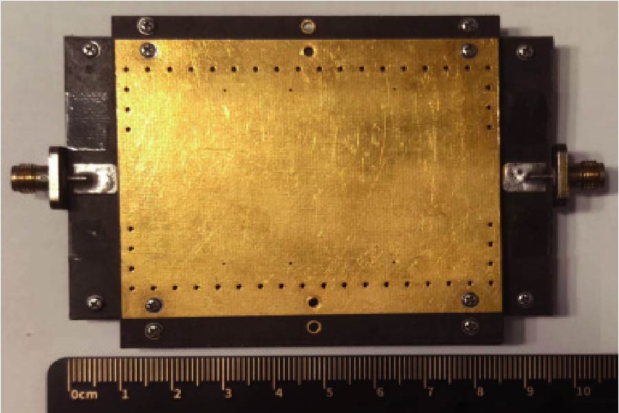
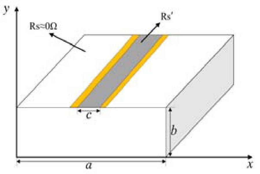
A low-cost and mechanical reconfigurable substrate integrate waveguide (SIW) equalizer is presented and studied in this work. Different from the previous SIW equalizers using Tantalum Nitride (TaN) or absorbing material as the resistive element, the indium tin oxides (ITO) are introduced into SIW equalizer. The absorbing material will deform under uneven pressure due to the structural softness of material, resulting in instable equalizing values. Compared with the absorbing material, ITO provides more structural stability, excellent high frequency characteristic, and can be easily integrated with traditional printed circuit board (PCB). Furthermore, an equalizer with reconfigurable equalizing values can be realized by adjusting ITO materials with different impedances. A SIW equalizer based on the ITO Conductive Film, operating from 26 to 40 GHz, has been designed, fabricated and experimentally verified. For measurement results, the return losses are better than -17.4 dB with 3, 6, and 10 dB equalizing values respectively over the entire Ka-band, and the insertion losses at the frequency point of 40 GHz are -2.89 dB, -4.80 dB, and -7.37 dB, respectively. The proposed equalizer presents the advantages of mechanical reconfigurable, low cost, and high stability. In addition, ITO Conductive Film is a good candidate for the design of high millimeter-wave band equalizer.
Low-Cost Substrate Integrated Waveguide Equalizer Based on the Indium Tin Oxides Conductive Film
2023-03-28
PIER Letters
Vol. 110, 11-19, 2023
download: 107
Reconfigurable Bandstop Filter with Switchable CLLs for Bandwidth Control
Moheddine Smari , Saber Dakhli , Erwan Fourn and Fethi Choubani
In this paper, a compact reconfigurable bandstop filter suitable for multistandard and multiband mobile terminals is reported. The proposed dual bandstop filter consists of a microstrip line coupled to two switchable Capacitively Loaded Loops (CLLs). We achieve tuning of individual notched frequency bands by using open circuits as switches and incorporated in each CLL element. The performance characteristics in terms of S-parameters and surface currents distribution show that the proposed filter is able to adjust two stopbands independently in a wide tuning range. A corresponding prototype of tunable dual-stopband filter is manufactured, and practical measurement agree well with the simulation results.
Reconfigurable Bandstop Filter with Switchable CLLs for Bandwidth Control
2023-03-25
PIER Letters
Vol. 110, 1-10, 2023
download: 114
Performance Optimization of Optical Access Networks Using Two Optical Amplifiers EYDWA and SOA in Cascade
Belabbes Berrahal , Amina Bendaoudi and Zoubir Mahdjoub
This work aims to evaluate the contribution of cascaded optical amplifiers in improving the performance of optical communication systems in optical access networks. This study is thus carried out by a system simulation software which presents results concerning the characteristic parameters of two optical amplifiers, EYDWA (Erbium Ytterbium Doped Waveguide Amplifier) and SOA (Semiconductor Optical Amplifier) used in cascade, namely their gains, the length of the guide and the concentration of ions.
Performance Optimization of Optical Access Networks Using Two Optical Amplifiers EYDWA and SOA in Cascade