A Novel Lumped LC Resonator Antenna with Air-Substrate for 5G Mobile Terminals
Shahanawaz Kamal,
Abdullahi S. B. Mohammed,
Mohd Fazil Ain,
Fathul Najmi,
Roslina Hussin,
Zainal Arifin Ahmad,
Ubaid Ullah,
Mohammadariff Othman and
Mohd Fariz Ab Rahman
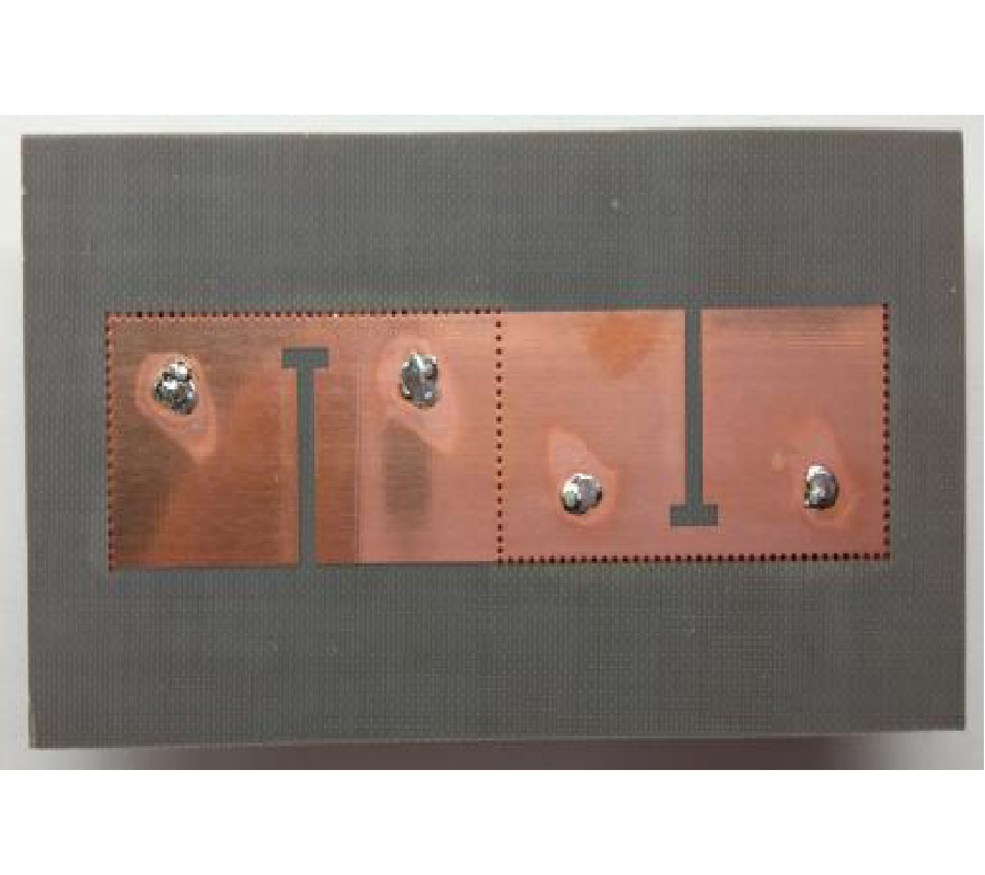
The extending applications for mobile computing have experienced immense progress over the previous decade. However, this has ultimately influenced the shortage of bandwidth. Therefore, to fulfill the consumers' demand, inexpensive antennas need to be uniquely designed for the next/fifth generation (5G) frequency spectrum. Consequently, this paper presents a novel antenna composed of inductors (L) or capacitors (C) on an air-substrate. Zinc (Zn) and copper (Cu) materials are utilized to fabricate the lumped LC resonator prototype. The effects of antenna's and substrate's thickness on resonant frequency or bandwidth have been studied. The finalized configuration engaged 1113 sq. mm area and operated at 28 GHz with approximately 3 GHz bandwidth. At resonant frequency, the system demonstrates peak gain and efficiency values of 10.6 dBi and 91%, respectively. The core objective of this paper is to report an antenna featuring simple and economical design along with premium results for 5G mobile terminals.