Vol. 1
Latest Volume
All Volumes
PIERL 110 [2023] PIERL 109 [2023] PIERL 108 [2023] PIERL 107 [2022] PIERL 106 [2022] PIERL 105 [2022] PIERL 104 [2022] PIERL 103 [2022] PIERL 102 [2022] PIERL 101 [2021] PIERL 100 [2021] PIERL 99 [2021] PIERL 98 [2021] PIERL 97 [2021] PIERL 96 [2021] PIERL 95 [2021] PIERL 94 [2020] PIERL 93 [2020] PIERL 92 [2020] PIERL 91 [2020] PIERL 90 [2020] PIERL 89 [2020] PIERL 88 [2020] PIERL 87 [2019] PIERL 86 [2019] PIERL 85 [2019] PIERL 84 [2019] PIERL 83 [2019] PIERL 82 [2019] PIERL 81 [2019] PIERL 80 [2018] PIERL 79 [2018] PIERL 78 [2018] PIERL 77 [2018] PIERL 76 [2018] PIERL 75 [2018] PIERL 74 [2018] PIERL 73 [2018] PIERL 72 [2018] PIERL 71 [2017] PIERL 70 [2017] PIERL 69 [2017] PIERL 68 [2017] PIERL 67 [2017] PIERL 66 [2017] PIERL 65 [2017] PIERL 64 [2016] PIERL 63 [2016] PIERL 62 [2016] PIERL 61 [2016] PIERL 60 [2016] PIERL 59 [2016] PIERL 58 [2016] PIERL 57 [2015] PIERL 56 [2015] PIERL 55 [2015] PIERL 54 [2015] PIERL 53 [2015] PIERL 52 [2015] PIERL 51 [2015] PIERL 50 [2014] PIERL 49 [2014] PIERL 48 [2014] PIERL 47 [2014] PIERL 46 [2014] PIERL 45 [2014] PIERL 44 [2014] PIERL 43 [2013] PIERL 42 [2013] PIERL 41 [2013] PIERL 40 [2013] PIERL 39 [2013] PIERL 38 [2013] PIERL 37 [2013] PIERL 36 [2013] PIERL 35 [2012] PIERL 34 [2012] PIERL 33 [2012] PIERL 32 [2012] PIERL 31 [2012] PIERL 30 [2012] PIERL 29 [2012] PIERL 28 [2012] PIERL 27 [2011] PIERL 26 [2011] PIERL 25 [2011] PIERL 24 [2011] PIERL 23 [2011] PIERL 22 [2011] PIERL 21 [2011] PIERL 20 [2011] PIERL 19 [2010] PIERL 18 [2010] PIERL 17 [2010] PIERL 16 [2010] PIERL 15 [2010] PIERL 14 [2010] PIERL 13 [2010] PIERL 12 [2009] PIERL 11 [2009] PIERL 10 [2009] PIERL 9 [2009] PIERL 8 [2009] PIERL 7 [2009] PIERL 6 [2009] PIERL 5 [2008] PIERL 4 [2008] PIERL 3 [2008] PIERL 2 [2008] PIERL 1 [2008]
2007-12-25
PIER Letters
Vol. 1, 263-273, 2008
download: 106
Tunnel Diode Integrated E-Shaped Patch Antenna for Broadband Operation
Jamshed Ansari Ram Ram
A tunnel diode integrated E-shaped patch antenna is proposed and analyzed using equivalent circuit concept. It is found that bias voltage of tunnel diode controls the performance of the antenna. Various tunable frequency bands are obtained by selecting suitable bias voltage while antenna topology remains unchanged. Bandwidth of the tunnel diode integrated patch improves to 40.26% over the 32.58% bandwidth of the patch. The radiation pattern also varies with bias voltage and a considerable improvement in beamwidth is observed however radiated power remains almost same.
TUNNEL DIODE INTEGRATED E-SHAPED PATCH ANTENNA FOR BROADBAND OPERATION
2007-12-25
PIER Letters
Vol. 1, 255-261, 2008
download: 234
Wideband Omnidirectional Operation Monopole Antenna
Yung-Tao Liu Che-Wei Su
This paper presents a square cylindrical monopole antenna easily fabricated using a cross-shaped metal plate for wideband omnidirectional operation. A prototype of the proposed antenna with a cross-sectional area of 8 × 8mm2 is implemented, and the antenna provides a wide operating bandwidth of about 7.5 GHz (1.8-9.4 GHz here), making it very promising for WMAN operation with the 802.16e standard in the 2 to 6 GHz. In addition, over the operating bandwidth, the antenna shows very good omnidirectional radiation patterns.
WIDEBAND OMNIDIRECTIONAL OPERATION MONOPOLE ANTENNA
2007-12-22
PIER Letters
Vol. 1, 245-254, 2008
download: 132
A Novel Design of Arbitrary Shaped Cells for Efficient Coverage from High Altitude Platforms
Yasser Albagory
This paper proposes a novel beamforming technique to form an arbitrary-shaped cell for the high altitude platforms (HAPs) mobile communications. The new technique is based on pattern summation of individual low-sidelobe narrow-beams which constitute the desired cell pattern weighted by an amplitude correcting function. The new cell pattern can be adapted to cover the main highways forming worm-shaped cells which may cover the highway for long distances up 100km and it will has an important role in reducing frequent handoffs and signaling traffic of location updating from moving users over the long highways.
A NOVEL DESIGN OF ARBITRARY SHAPED CELLS FOR EFFICIENT COVERAGE FROM HIGH ALTITUDE PLATFORMS
2007-12-21
PIER Letters
Vol. 1, 237-243, 2008
download: 158
Electronic Spectrum Study of Parabolic GaAs /Al_{X}Ga_{1-X}as Superlattices
Isaac Rodríguez-Vargas O. Y. Sanchez-Barbosa David Armando Contreras-Solorio Stoyan Vlaev
The electronic structure of finite parabolic GaAs/AlxGa1-xAs superlattices is studied. A detailed analysis of the miniband formation is given and the importance of all system parameters is discussed. The dependence of the equidistant miniband separation on the superlattice size is revealed. A comparison with different theoretical methods and experimental data is presented. The calculations are conducted in the framework of the semi-empirical sp3s* tight-binding model including spin applying the Green function formalism and the Surface Green Function Matching Method (SGFM) method.
ELECTRONIC SPECTRUM STUDY OF PARABOLIC GAAS/AL_{X}GA_{1-X}AS SUPERLATTICES
2007-12-19
PIER Letters
Vol. 1, 221-235, 2008
download: 139
Scattering Field for the Ellipsoidal Targets Irradiated by an Electromagnetic Wave with Arbitrary Polarizing and Propagating Direction
Ying-Le Li Ji-Ying Huang Ming-Jun Wang Jiatian Zhang
Obtaining scattering field for an ellipsoid irradiated by electromagnetic wave with arbitrary polarizing and propagating direction is a hard topic that has caused large attention in the world. Literatures relative to it are seldom found. In this paper, the scattering field for an ellipsoid is presented by utilizing the scales transformation of electromagnetic field and coordinate system rotation, as the incident wave irradiating the target with arbitrary polarizing and propagating direction. The result obtained is in good agreement with that in the reference when all the scale factors changes into 1. We take a conductor ellipsoid as an example, simulations both for ellipsoid and plant leaf are presented respectively by way of choosing the different scale factor. Results show that the scattering field is sensitively affected by polarization of the incident wave and varies not too greatly with the incident wave and changes with the observing point. At some points the scattering energy arrives to its maximum.
SCATTERING FIELD FOR THE ELLIPSOIDAL TARGETS IRRADIATED BY AN ELECTROMAGNETIC WAVE WITH ARBITRARY POLARIZING AND PROPAGATING DIRECTION
2007-12-13
PIER Letters
Vol. 1, 205-210, 2008
download: 114
Numerical Method of Simulation of Material Influences in Mr Tomography
Miloslav Steinbauer Radek Kubasek Karel Bartusek
Generally all Magnetic Resonance Imaging (MRI) techniques are affected by magnetic and electric properties of measured materials, resulting in errors in MR image. Using numerical simulation we can solve the effect of changes in homogeneity of static and RF magnetic fields caused by specimen made from conductive and/or magnetic material in MR tomograph. This paper deals with numerical simulation of material susceptibility influence to magnetic field.
NUMERICAL METHOD OF SIMULATION OF MATERIAL INFLUENCES IN MR TOMOGRAPHY
2007-12-13
PIER Letters
Vol. 1, 197-204, 2008
download: 206
Latest Trends in Millimeter-Wave Imaging Technology
Soichi Oka Hiroyoshi Togo Naoya Kukutsu Tadao Nagatsuma
This paper overviews the latest trends of millimeterwave (MMW) imaging technologies, focusing mainly on applications of and technical parameter variations for security surveillance and nondestructive inspections (NDI).We introduce a smart NDI tool using active W-band imaging, which is capable of detecting hidden surface cracks in concrete structures.
LATEST TRENDS IN MILLIMETER-WAVE IMAGING TECHNOLOGY
2007-12-12
PIER Letters
Vol. 1, 189-196, 2008
download: 283
Analysis of Capacitance Across Interconnects of Low-k Dielectric Used in a Deep Sub-Micron CMOS Technology
Sonanvane Avinash Bhavana N. Joshi Ashok Mahajan
The paper presents the detailed analysis of the interconnect capacitance, crosstalk time and peak crosstalk voltage. The dependency of the couple capacitance and fringe capacitance on the interconnect layer dimensions affects significantly to the interconnect capacitance. The peak crosstalk time obtained to be 13 femtoseconds for 9.6 femtoseconds of propagation delay, while the maximum crosstalk voltage obtained to be 178 mV.
ANALYSIS OF CAPACITANCE ACROSS INTERCONNECTS OF LOW-K DIELECTRIC USED IN A  DEEP SUB-MICRON CMOS TECHNOLOGY
2007-12-12
PIER Letters
Vol. 1, 181-188, 2008
download: 111
3D Microstructuring of Glass by Femtosecond Laser Direct Writing and Application to Biophotonic Microchips
Koji Sugioka Yasutaka Hanada Katsumi Midorikawa
Three-dimensional (3D) microfabrication of photostructurable glass by femtosecond (fs) laser direct writing is demonstrated for manufacture of biophotonic microchips. The fs laser direct writing followed by annealing and successive wet etching can fabricate the hollow microstructures, achieving a variety of microfluidic components and microoptical components in a glass chip. One of the interesting and important applications of the 3D microfluidic structures fabricated by the present technique is inspection of living microorganisms. The microchips used for this application are referred to as nanoaquarium. Furthermore, the optical waveguide is written inside the glass by the fs laser direct writing without the annealing and the successive etching. It is revealed that integration of the microfluidic and microoptical components with the optical waveguides in a single glass chip is of great use for biochemical analysis and medical inspection based on optical sensing.
3D MICROSTRUCTURING OF GLASS BY FEMTOSECOND LASER DIRECT WRITING AND APPLICATION TO BIOPHOTONIC MICROCHIPS
2007-12-12
PIER Letters
Vol. 1, 173-179, 2008
download: 116
An Example of Holographic Radar Using at Restoration Works of Historical Building
Vladimir Razevig Sergey Ivashov Anton Sheyko Igor Vasilyev Andrey Zhuravlev
The former Senate building, Saint-Petersburg, Russia is being refitted for using it by the Constitutional court of Russian Federation. The team of Remote Sensing Laboratory was invited to participate in this work. The case is that the underfloor water heating system had been installed in the Senate building. The arrangement of pipes hasn't been precisely documented. Besides, there are power and communications cables as well as metal mesh under the concrete floor of the building. Workers were afraid of damaging pipes and cables during laying the parquet floor. Main purpose was to investigate the building floor and to define exact position of pipes and cables with the help of subsurface holographic radars developed by Remote Sensing Laboratory.
AN EXAMPLE OF HOLOGRAPHIC RADAR USING AT RESTORATION WORKS OF HISTORICAL BUILDING
2007-12-10
PIER Letters
Vol. 1, 167-172, 2008
download: 120
Enhancement of the Electronic Confinement Improves the Mobility in P-n -P Delta-Doped Quantum Wells in Si
Augusto Ariza-Flores Isaac Rodríguez-Vargas
The electronic structure and mobility trends in a n-type delta-doped quantum well in Si, matched between p-type delta-doped barriers of the same material, is presented. The distance between the n-type well and p-type barriers is varied from 50A to 500A; and also the impurity density from 5 × 1012 cm-2 to 5 × 1013 cm-2, for both, donors and acceptors. An increase in the mobility by a factor of 1.6 at interwell distance of 50A with donor and acceptor concentrations of 5 × 1012 cm-2 and 5 × 1013 cm-2 compared with a single delta-doped well without p-type barriers is found. This improvement in mobility could be attributed to a better confinement of carriers, which favors excited levels with nodes in the donor plane. This trade-off between carrier concentration and mobility could be exploited in high-speed, high-power and high-frequency applications.
ENHANCEMENT OF THE ELECTRONIC CONFINEMENT IMPROVES THE MOBILITY IN P-N-P DELTA-DOPED QUANTUM WELLS IN SI
2007-12-10
PIER Letters
Vol. 1, 159-165, 2008
download: 109
Electron Subband Structure and Mobility Trends in P-n Delta-Doped Quantum Wells in Si
Augusto Ariza-Flores Isaac Rodríguez-Vargas
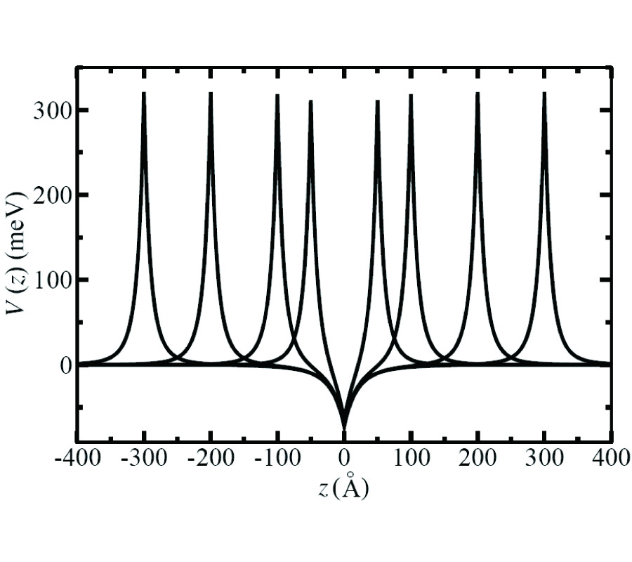
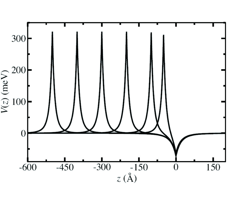
We present the electronic spectrum of a n-type deltadoped quantum well in Si coupled to a p-type delta-doped barrier within the envelope function effective mass approximation. We applied the Thomas-Fermi approximation to derive an analytical expression for the confining potential, and thus, we obtain the electronic structure in a simple manner. We analyzed the electron subband structure varying the distance between the doping planes (l) as well as the impurity density in them (n2D, p2D). We also study the mobility trends through an empirical formula that is based on the electron levels, the electron wave functions and the Fermi level. We find a monotonic decrease in the mobility as the p-type barrier moves away from the n-type well, and optimum parameters, l = 70A and n2D = 5 × 1012 cm-2 and p2D = 5×1013 cm-2, for maximum mobility.
ELECTRON SUBBAND STRUCTURE AND MOBILITY TRENDS IN P-N DELTA-DOPED QUANTUM WELLS IN SI
2007-12-08
PIER Letters
Vol. 1, 149-158, 2008
download: 99
An Analytic Formula of the Current Distribution for the VLF Horizontal Wire Antenna Above Lossy Half-Space
Hai Chen Jian-Xin Luo Da-Kui Zhang
An analytical formula of the current distribution for the VLF horizontal wire antenna located above the ground is presented in this paper. This formula is suitable for the VLF horizontal antenna which is fed at arbitrary position and with arbitrary loaded impedance at the end. In order to validate the analytical formula, a numerical code based on MoM is also developed. The comparison between the results obtained by two methods proves the validity of the analytical formula proposed in this paper.
AN ANALYTIC FORMULA OF THE CURRENT DISTRIBUTION FOR THE VLF HORIZONTAL WIRE ANTENNA ABOVE LOSSY HALF-SPACE
2007-12-08
PIER Letters
Vol. 1, 139-148, 2008
download: 112
Strong Geomagnetic Disturbances and Induced Currents on Earth Surface
Ana Elias V. Silbergleit
Long-term variations in strong geomagnetic storms are analyzed and linked to electric fields induced on Earth. In fact, geomagnetic disturbances generate electric fields that drive currents in the Earth which may have significant effects on electrical systems and pipelines. The present study will be carried out using aa, AE and Dst index data to estimate long-term variations in strong geomagnetic disturbances. The results are extended then to the space weather topic through a rough assessment of the expected Earth electric field from measured horizontal components of the surface magnetic field, and also through a qualitative estimation of the consequent currents and voltages induced in a pipeline using the distributed source transmission line (DSTL) theory.
STRONG GEOMAGNETIC DISTURBANCES AND INDUCED CURRENTS ON EARTH SURFACE
2007-12-04
PIER Letters
Vol. 1, 129-138, 2008
download: 644
Improving the Performance of an Antenna Array by Using Radar Absorbing Cover
Abdelmonem Abdelaziz
Improving the performance of a microstrip antenna array has been considered based on the innovative use of an absorbing radar cover.Since the surface wave between antennas array elements plays a major role in mutual coupling and scattering behavior of array antenna. The main objective of this work is to reduce the effect of surface wave between array elements using radar absorbing cover.The absorbing cover has been designed with spatial configuration to get maximum performance at the resonant frequency of the fabricated microstrip antenna array.The measured results of the tested antenna array show a significant reduction of both mutual coupling between array patches and radar cross section of the tested antenna array with minimum side effects on the antenna parameters.
IMPROVING THE PERFORMANCE OF AN ANTENNA ARRAY
BY USING RADAR ABSORBING COVER
2007-12-02
PIER Letters
Vol. 1, 119-128, 2008
download: 166
Analysis of Wavefunction Distribution in Quantum Well Biased Laser Diode Using Transfer Matrix Method
Edmund Samuel Dyneshwar Patil
The paper presents the faster, simpler, and accurate algorithm to solve time independent Schrodinger equation based on transfer matrix method. We can thus calculate all bound and quasi bound energy and the corresponding probability density. A central part of this paper deals with the solving of Schrodinger equation for quantum well structure. Our results show that the transfer matrix method is accurate, it is easier to implement. The increase in well width increases the FWHM from 5.4 nanometer to 9.4 nanometer, while the increase in the Aluminum concentration the FWHM decreases from 8.98 to 5.4.
ANALYSIS OF WAVEFUNCTION DISTRIBUTION IN QUANTUM WELL BIASED LASER DIODE USING TRANSFER MATRIX METHOD
2007-12-02
PIER Letters
Vol. 1, 109-118, 2008
download: 394
The Classical Structure Model of Single Photon and Classical Point of View with Regard to Wave-Particle Duality of Photon
Dong-Lin Zu
The enigma of the wave-particle duality of photon has remained unimpressively explained for a century since Einstein presents the concept of the photon in 1905. This article establishes a classical geometric structure model of a single photon based on field matter, educes a formula for the size of a photon; assumes that there only are two kinds of photon of right hand and left hand circular polarized, and suggests the frequency ω of photon polarization rotated to be its spin frequency. It ascribes the wavelike of photon to its spin motion and the particle-like to its translation motion. From the point of photon particle instead of wave view to re-analyze Young's double-slit interference and polarizer experiments, gives reasonable mechanism. It defines the phase velocity and the group velocity of a photon. It gives a unified and consistent understanding of quantum particle of light and classical electromagnetic waves field. Evidently, such a precisely defined conceptual model is reasonable, objective and easy to accept for classical physicists.
THE CLASSICAL STRUCTURE MODEL OF SINGLE PHOTON AND CLASSICAL POINT OF VIEW WITH REGARD TO WAVE-PARTICLE DUALITY OF PHOTON
2007-11-28
PIER Letters
Vol. 1, 101-108, 2008
download: 141
A Novel Ultra-Wideband Bow-Tie Slot Antenna in Wireless Communication Systems
Yan-Lin Chen Cheng-Li Ruan Lin Peng
A novel ultra-wideband bow-tie slot antenna fed by CPW is proposed in this paper. This antenna has been demonstrated to provide an UWB with return loss less than -10 dB from 9.5 GHz to 22.4 GHz. The bandwidth is up to 80%, which is quite better than the traditional bow-tie slot antenna. Simulated and measured results are presented.
A NOVEL ULTRA-WIDEBAND BOW-TIE SLOT ANTENNA IN WIRELESS COMMUNICATION SYSTEMS
2007-11-28
PIER Letters
Vol. 1, 93-99, 2008
download: 331
Reflection and Transmission in the Ionosphere Considering Collisions in a First Approximation
Ali Yesil Mehmet Aydogdu Ana Elias
Reflection and transmission coefficients (R and T) of high frequency waves propagating in the ionosphere are studied taking collisions into account. This was done approximating the expression (1 + Z2)-1 in the refractive index using binomial expansion and neglecting terms of order higher than Z2, where Z is the ratio between the electron collision frequency and the wave frequency. R and T height profiles were assessed using the International Reference Ionosphere, IRI, to estimate the ionosphere plasma parameters. Although no significant differences are found between the estimation with and without collisions, the method employed to include collisions may be useful for other purposes where collisions should be taken into account.
REFLECTION AND TRANSMISSION IN THE IONOSPHERE CONSIDERING COLLISIONS IN A FIRST APPROXIMATION
2007-11-27
PIER Letters
Vol. 1, 85-92, 2008
download: 335
Analysis of Electrically Small Size Conical Antennas
Yu Yu Kyi Jian-Ying Li
It has long been known that the conical antenna has broadband characteristics and good radiation efficiency. The design considerations in reducing the size of top loaded conical antenna by using posts with lumped resistive loading are presented. The resulting antenna can achieve a VSWR of better than 2.0 over 100-800MHz frequency range. Results indicate that the addition of posts and lumped resistive loading has significant role in designing broadband antennas which are in small size.
ANALYSIS OF ELECTRICALLY SMALL SIZE CONICAL ANTENNAS