A Circular Sector with an Inverted L Shaped Monopole Antenna for Tri-Band Applications
Alka Khade ,
Mahadu Trimukhe ,
Shishir Jagtap and
Rajiv Kumar Gupta
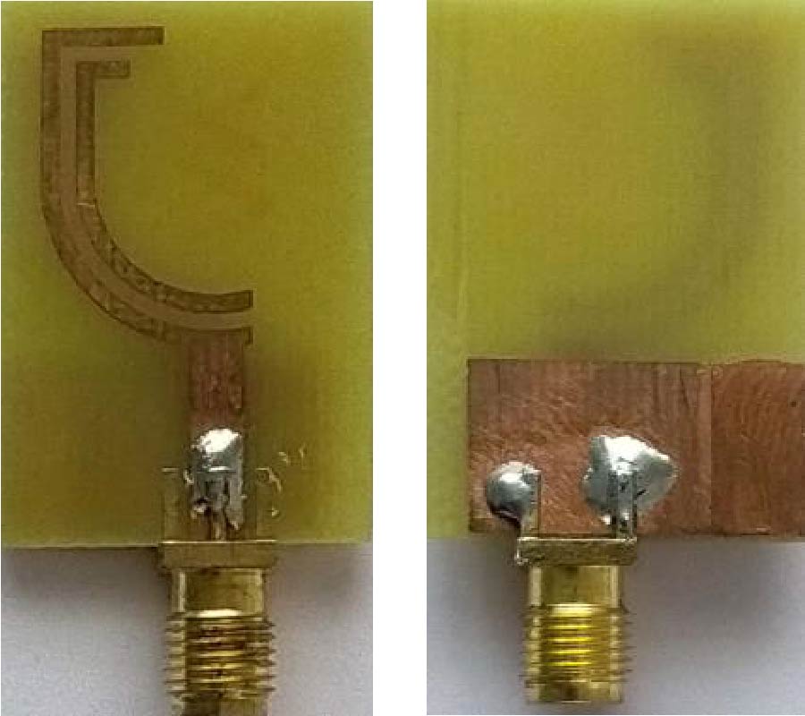
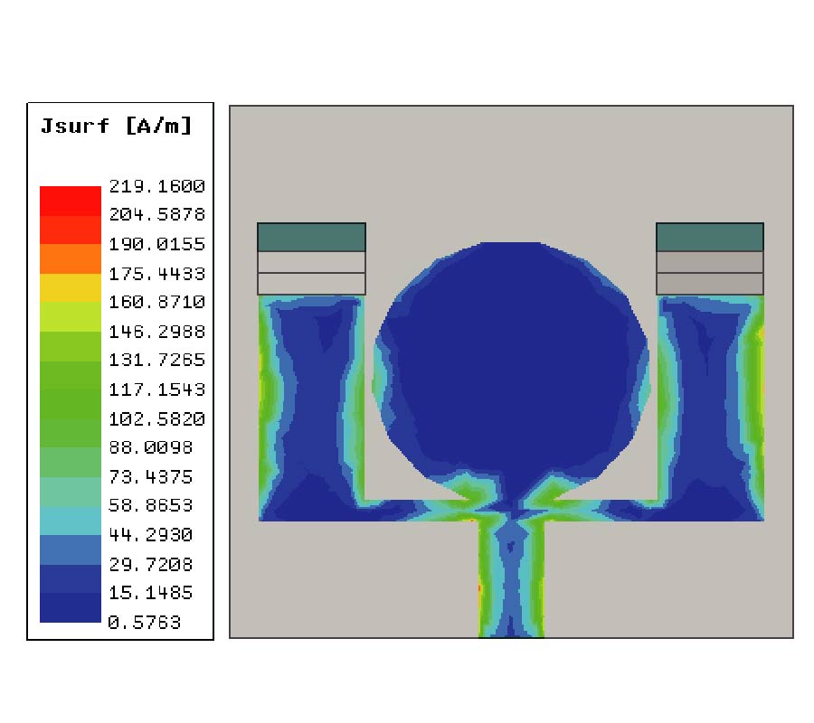
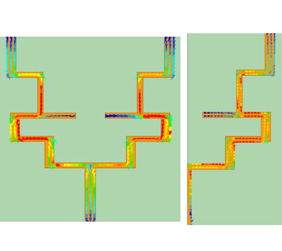
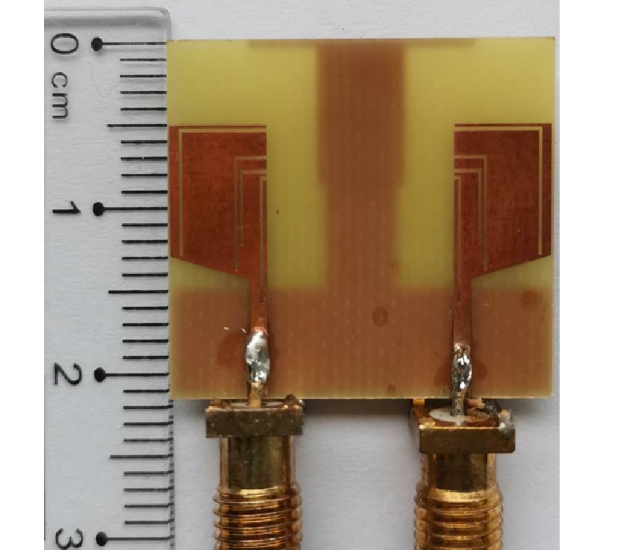
In this paper, a quarter circular sector with an inverted L shaped monopole antenna for tri-band applications is proposed. The antenna is designed from a U shaped ultra-wideband (UWB) antenna. The number of higher-order modes, each with wide bandwidth, gets excited in a monopole, which electromagnetically couple to provide UWB. In the proposed tri-band antenna the electromagnetic coupling between higher-order modes is reduced by selectively removing the symmetrical portion and decreasing the thickness of the UWB radiator. An inverted L strip is added to a quarter circular sector, and a similarly shaped parasitic element is placed close to the radiator to achieve the desired tri-band. The antenna provides S11 ≤ -10 dB over 2.1-2.5 GHz, 5.0-5.6 GHz and 8.4-9.0 GHz which covers 3G, Wi-Fi, LTE, Bluetooth, WLAN and X- band applications. The antenna offers nearly omnidirectional radiation pattern in the lower band and directional radiation pattern in the other two bands, The prototype antenna is fabricated on a 0.147λ0×0.22λ0 FR4 substrate, where λ0 is the free-space wavelength corresponding to 2.1 GHz. The measured results agree with simulation ones.