Search Results(14087)

2010-08-04
PIER
Vol. 107, 161-178
A d -Band Power Amplifier with 30-GHz Bandwidth and 4.5-dBm Psat for High-Speed Communication System
Bo Zhang , Yong-Zhong Xiong , Lei Wang , Sanming Hu , Teck-Guan Lim , Yi-Qi Zhuang and Joshua Le-Wei Li
This paper presents a D-band power amplifier for high-speed communication system. The capacitive effect of interconnection via on transistor performance at high frequency is analyzed and a new via structure is employed to reduce the capacitive effect. The on-chip matching technique for high frequency amplifier is analyzed and the thin-film microstrip line matching network is used, which is combined with biasing network to reduce RF signal loss and silicon cost. The amplifier is fabricated in 0.13-μm SiGe BiCMOS process. The experimental results show a 7 dB gain at 130 GHz with 3-dB bandwidth of 30-GHz. The input return loss is better than 10 dB over 23 GHz. In addition, this amplifier achieves saturated output power (Psat) of 4.5 dBm and input 1-dB gain compression point (P1dB) of -4.5 dBm. The chip size of implemented power amplifier is only 0.22mm2.
A D-BAND POWER AMPLIFIER WITH 30-GHZ BANDWIDTH AND 4.5-DBM PSAT FOR HIGH-SPEED COMMUNICATION SYSTEM
2010-08-04
PIER
Vol. 107, 147-159
A Novel Approach for RCS Reduction Using a Combination of Artificial Magnetic Conductors
María Elena de Cos Gómez , Yuri Alvarez-Lopez and Fernando Las Heras Andres
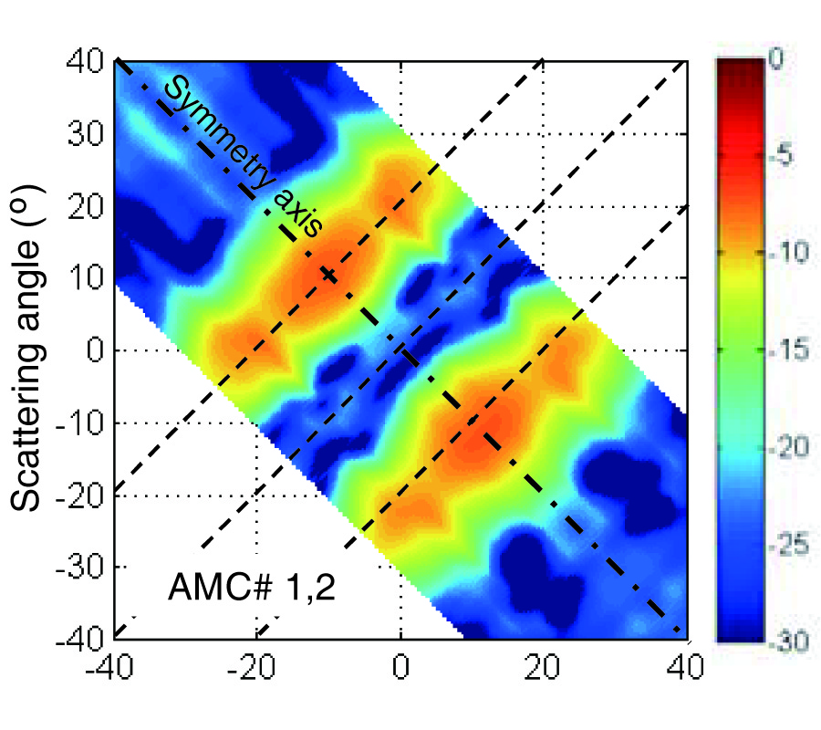
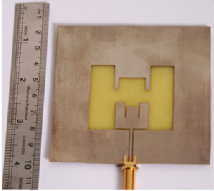
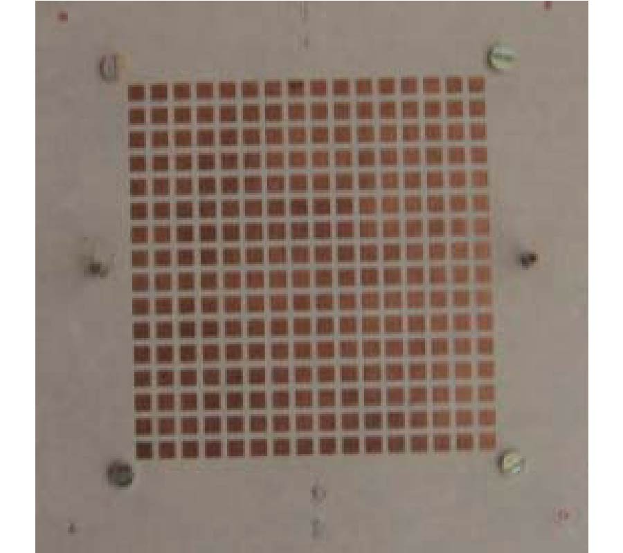
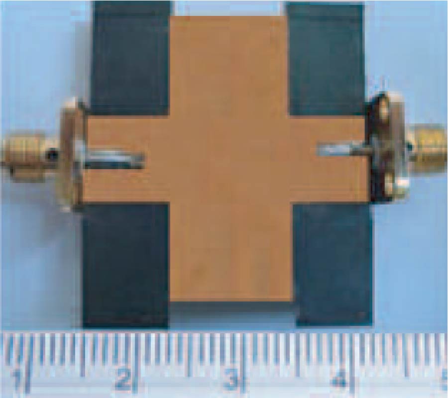
A thin Artificial Magnetic Conductor (AMC) structure for Radar Cross-Section (RCS) reduction applications is presented. The manufactured prototype, which combines two unit-cell metallization sizes, presenting two resonant frequencies, shows broad AMC operation bandwidth, polarization angle independency, and its angular margin when operating under oblique ncidence is also tested. It is shown that significant RCS reduction can be achieved with the proposed AMCs combination even if a 180º phaseshift between reflected waves is not met. Two designs are considered: the already mentioned design combining AMCs with overlapped frequency bands and the second one combining Perfect Electric Conductor (PEC) and AMC surfaces. A comparison between these two designs regarding RCS reduction, supported by measurements in an anechoic chamber, is presented.
A NOVEL APPROACH FOR RCS REDUCTION USING A COMBINATION OF ARTIFICIAL MAGNETIC CONDUCTORS
2010-08-04
PIER
Vol. 107, 129-146
Efficient Time-Domain Noise Modeling Approach for Millimeter-Wave Fets
Shahrooz Asadi and Mustapha C. E. Yagoub
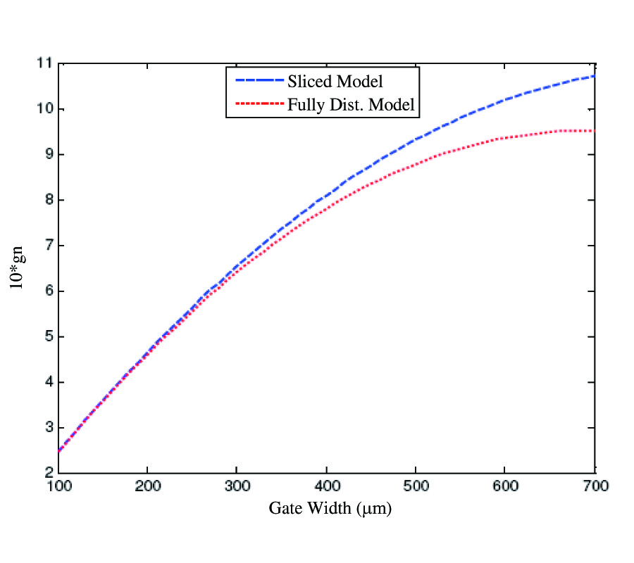
Based on the active coupled line concept, a novel approach for efficient noise performance modeling of millimeter-wave field-effect transistors is proposed. This distributed model considers the effect of wave propagation along the device electrodes, which can significantly affect the noise performance especially in the millimeter-wave range. By solving the multi-conductor transmission line equations, using the Finite-Difference Time-Domain technique, this procedure can accurately determine the noise correlation matrix of the transistor and then its noise performance.
EFFICIENT TIME-DOMAIN NOISE MODELING APPROACH FOR MILLIMETER-WAVE FETS
2010-08-03
PIER Letters
Vol. 16, 131-139
A Novel Compact UWB Antenna with 3.5/5.2/5.8 GHz Triple Band-Notched Characteristics
Li-Shi Ren , Fan Li , Jin-Juan Zhao , Gang Zhao and Yong-Chang Jiao
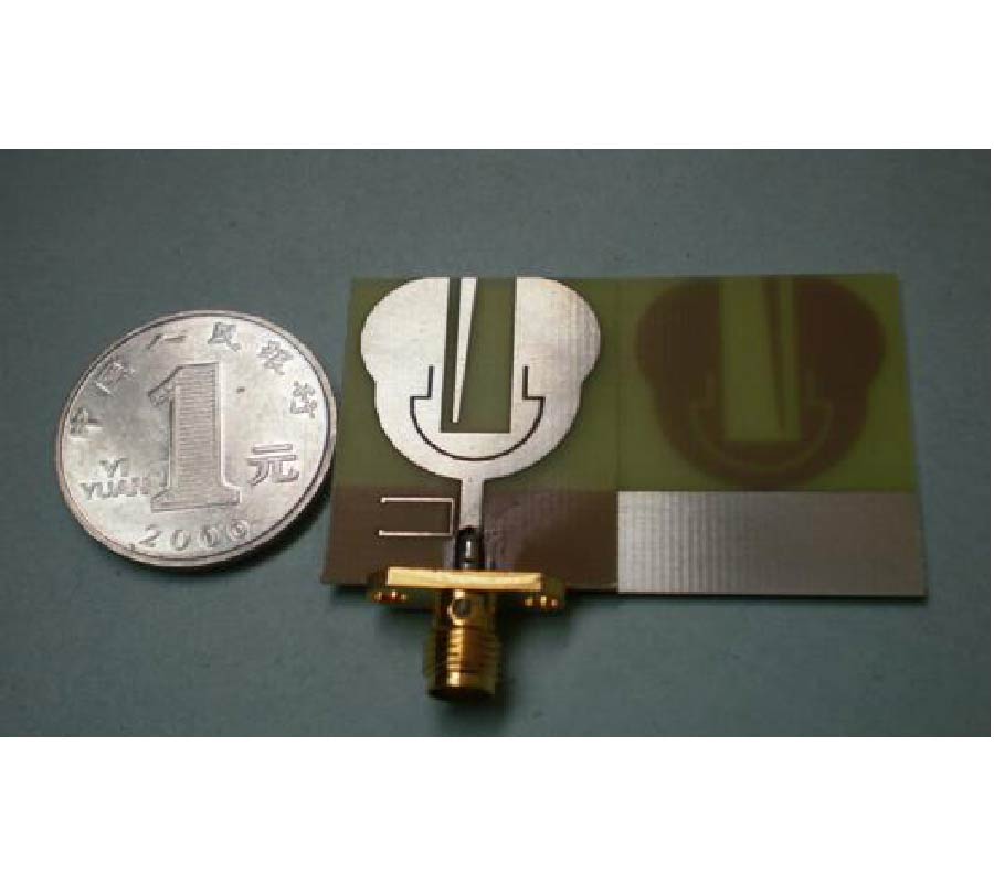
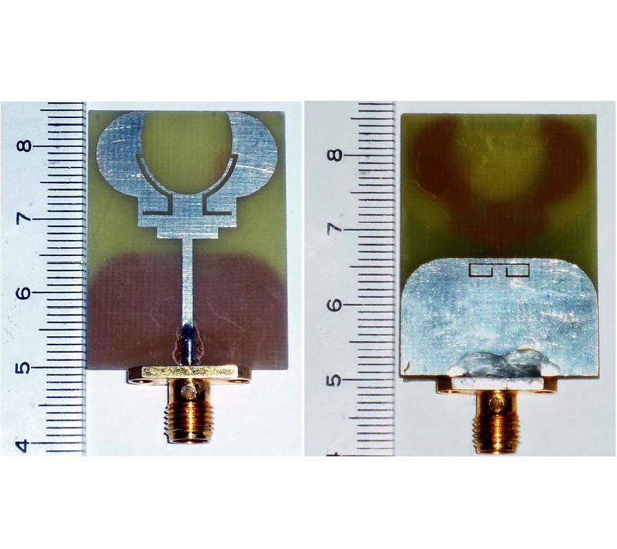
A novel compact fork-shaped ultrawideband (UWB) antenna with triple band-notched characteristics is proposed. By embedding a spade-shaped slot on the radiating patch as well as adding a separated strip and a C-shaped resonating structure on the front side of the reference UWB antenna, the triple notched frequency bands are realized. The measured impedance bandwidth defined by VSWR<2 of 7.8 GHz (3--10.8 GHz), with the triple notched bands of 3.3--3.7 GHz, 5.15--5.4 GHz, and 5.7--5.9 GHz, are obtained. The proposed antenna with an overall dimension of only 24×30 mm2 is successfully simulated, designed and measured, showing broadband matched impedance and stable radiation patterns.
A NOVEL COMPACT UWB ANTENNA WITH 3.5/5.2/5.8 GHz TRIPLE BAND-NOTCHED CHARACTERISTICS
2010-08-03
PIER Letters
Vol. 16, 119-129
Dual-Band Yagi-Uda Antenna for Wireless Communications
Qi Xin , Fu-Shun Zhang , Bao-Hua Sun , Yanlin Zou and Qi-Zhong Liu
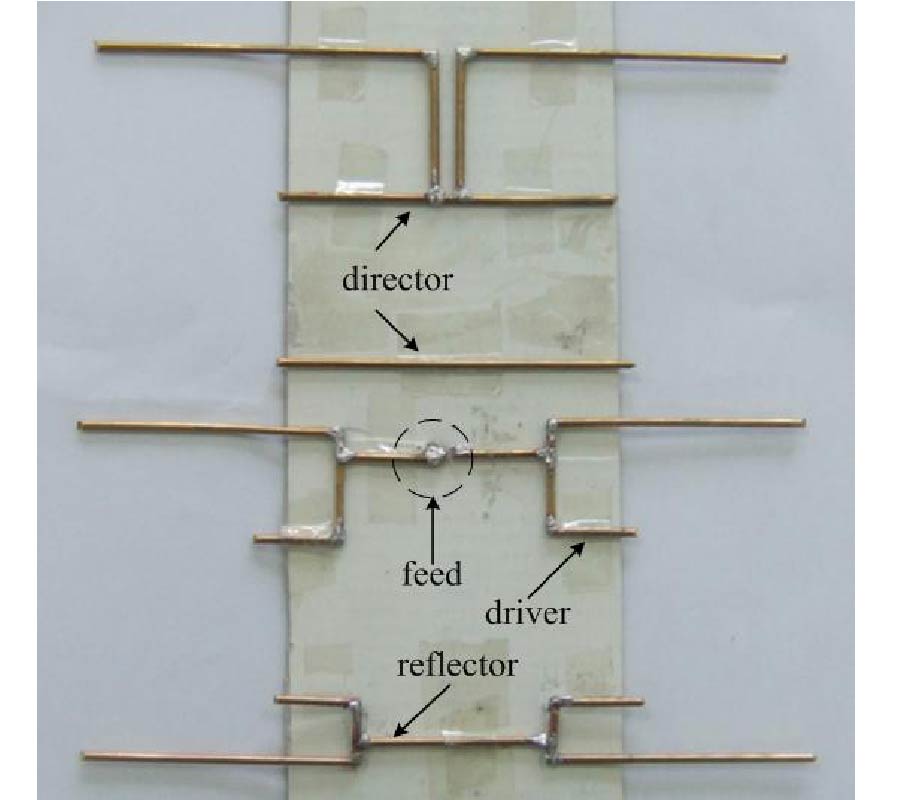
A novel Yagi-Uda antenna with dual-band (915-935MHz and 1760-1805MHz) is presented. Branch structures are used to realize dual-band performance. The geometrical parameters for the branch structures are optimized to explore the antenna to operate satisfactorily in the two bands. Prototype is manufactured and measured, and the results are in good agreement with the simulated ones. In the two operating bands, the proposed antenna achieves directional radiation and the performances that VSWR<2, gain 5-6.6 dBi and front-to-back ratio 6-9.1dB, making it suitable for the non-fixed base station backhaul in wireless communications.
DUAL-BAND YAGI-UDA ANTENNA FOR WIRELESS COMMUNICATIONS
2010-08-03
PIER Letters
Vol. 16, 109-117
A Novel Dual Band-Notched Monopole Antenna for Ultra-Wideband Application
Yang Zhu , Fu-Shun Zhang , Chen Lin , Qiang Zhang and Jing-Xiu Huang
In this article,a printed ultra-wideband (UWB) monopole antenna with dual band-notched characteristics of size 26 mm×35 mm is presented. The prototype consists of pincers-shaped radiation element and corner rounded ground plane. By inserting a pair of flexuous slots on the radiation element and a C-shaped slot on the ground plane, the 3.5/5.5 GHz dual band-notched characteristics are achieved, respectively. Moreover, good radiation patterns and gains within the operating band have been obtained. The detailed design and experimental results are discussed in this article.
A NOVEL DUAL BAND-NOTCHED MONOPOLE ANTENNA FOR ULTRA-WIDEBAND APPLICATION
2010-08-03
PIER C
Vol. 15, 89-101
Broadband Coplanar Waveguide-Fed Wide-Slot Antenna
Aliakbar Dastranj and Mehrzad Biguesh
A large bandwidth wide-slot antenna, fed by coplanar waveguide (CPW), is proposed. Experimental investigations and detailed simulations are conducted to understand its behavior and to optimize for broadband operation. The impedance bandwidth, determined by 10-dB return loss of the proposed slot antenna using both measurement and simulation, is about 131% (2.8 to 14 GHz). In addition to be small in size, the antenna has low cross polarization, relatively high gain, and it exhibits stable far-field radiation characteristics in the entire operating bandwidth. The design with very wide operating bandwidth and improved radiation pattern is obtained by properly choosing the suitable slot shape, selecting similar feed patch shape, and tuning their dimensions. Numerical sensitivity analysis has been used to understand the effects of changes of various antenna dimensions and to optimize the performance of the designed antenna. Based on our computer simulations it is shown that the antenna dimensions parameters have uncorrelated effects on the upper edge of the bandwidth. Simulation results show that the impedance matching of this kind of antenna is sensitive to the feed-slot combination and feed gap width. The simulated and measured results for return loss, far-field E-plane and H-plane radiation patterns, and gain of the designed antenna are presented and discussed.
BROADBAND COPLANAR WAVEGUIDE-FED WIDE-SLOT ANTENNA
2010-08-03
PIER
Vol. 107, 115-128
A New Defected Ground Structure and Its Application for Miniaturized Switchable Antenna
Jingxian Liu , Wen-Yan Yin and Sailing He
A new defected ground structure (DGS) is firstly proposed in this paper, which has better slow-wave effect than that of cross or dumbbell one. Using the model of transmission line, its equivalent parameters are extracted. With good omni-directional properties, the proposed DGS is then used in the design of a proximity coupled antenna for its miniaturization. The size of the developed antenna is about 68% smaller than that of the conventional one. Further, two artificial cells are added on the feed line to reduce the protrudent stub length from 26.9mm to 18.94 mm. With the utility of the DGS and artificial cells, the size of proximity coupled antenna is reduced significantly. By introducing a PIN diode at the end of feed line, the antenna is switchable in both x- and y-direction linear polarizations. Such miniaturization in antenna size has little negative effect on its cross polarization, with both simulated and experimental results presented for comparison.
A NEW DEFECTED GROUND STRUCTURE AND ITS APPLICATION FOR MINIATURIZED SWITCHABLE ANTENNA
2010-08-02
PIER C
Vol. 15, 75-87
A Stacked Ring-Patch Artificial Substrate to Improve the Antenna Performance
Menasinakaihosahalli Ningappa Sujatha and Kalarickaparambil Vinoy
In this paper, a stacked ring-patch two layer planar artificial substrate is analyzed numerically and is shown to possess the properties of a high impedance surfaces (HIS). Its properties are evaluated by investigating the surface wave propagation and plane wave reflection characteristics. Its application to reduce the mutual coupling of microstrip antennas and to improve the radiation pattern are investigated by simulation tool CST microwave studio. Experimental measurements using a pair of monopoles are used to confirm the surface waves suppression band. One of the main advantages of the proposed geometry is that it is simple and planar in nature, without the need for any via connections across dielectric layers and thus can be realized by planar technologies. Another advantage is that it exhibits over lapped surface wave suppression and in-phase reflection bands. Also it can be scalable to operate in different frequency range.
A STACKED RING-PATCH ARTIFICIAL SUBSTRATE TO IMPROVE THE ANTENNA PERFORMANCE
2010-08-02
PIER M
Vol. 13, 173-188
Artificial Neural Networks Approach in Microwave Filter Tuning
Jerzy Julian Michalski
This paper presents a novel method of cavity filter tuning with the usage of an artificial neural network (ANN). The proposed method does not require information on the filter topology, and the filter is treated as a black box. In order to illustrate the concept, a feed-forward, multi-layer, non-linear artificial neural network with back propagation is applied. The method for preparing, learning and testing vectors consisting of sampled detuned scattering characteristics and corresponding tuning screw deviations is proposed. To collect the training vectors, the machine, an intelligent automatic filter tuning tool integrated with a vector network analyzer, has been built. The ANN was trained on the basis of samples obtained from a properly tuned filter. It has been proved that the usage of multidimensional approximation ability of an ANN makes it possible to map the characteristic of a detuned filter reflection in individual screw errors. Finally, after the ANN learning process, the tuning experiment on 6 and 11-cavity filters has been preformed, proving a very high efficiency of the presented method.
ARTIFICIAL NEURAL NETWORKS APPROACH IN MICROWAVE FILTER TUNING
2010-08-02
PIER
Vol. 107, 101-114
Design of a High Band Isolation Diplexer for GPS and WLAN System Using Modified Stepped-Impedance Resonators
Ru-Yuan Yang , Chin-Min Hsiung , Cheng-Yuan Hung and Chih-Chin Lin
In this paper, we presented the design of a high performance diplexer for applications of global positioning system (GPS) at 1.575 GHz and wireless local area network (WLAN) at 2.4 GHz, simultaneously. Two bandpass filters (BPFs) using the modified stepped-impedance resonators (SIRs) operated at 1.575 GHz and 2.4 GHz are main blocks for the proposed diplexer. By discussing and analyzing the admittance of the even and odd modes, the transmission zero of the modified SIR can be found, and the location of the transmission zero can be precisely predicted, thus having a wide and deep stopband for the BPFs, in turn the high performance diplexer. Furthermore, due to the appearance of the transmission zeros near the passband edges, the passband selectivity of the BPFs as well as the diplexer can be improved. By using the impedance matching between two BPFs, a high isolation of 50 dB between two channels is obtained. The proposed diplexer was designed, fabricated and measured. The simulated and measured results had a good agreement with the proposed design concept.
DESIGN OF A HIGH BAND ISOLATION DIPLEXER FOR GPS AND WLAN SYSTEM USING MODIFIED STEPPED-IMPEDANCE RESONATORS
2010-08-01
PIER Letters
Vol. 16, 99-108
The Miniature Frequency Doubler Using Compensated Capacitive Line in Balun
Yu-Ann Lai , Chun-Nien Chen , Chun-Chi Su , Chih-Ming Lin and Yeong-Her Wang
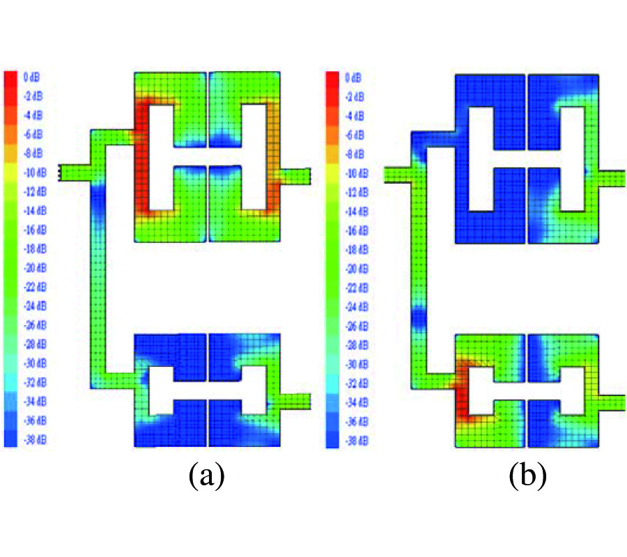
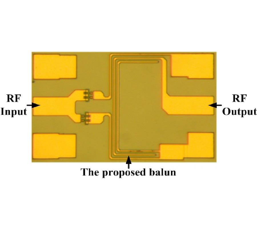
A compact balanced frequency MMIC doubler using compensated capacitive line in Marchand balun is proposed. With multi-coupled lines technology, the balun is applied to a balanced doubler successfully. Compared with the conventional Marchand balun, more than 55% reduction in the length of coupled line can be achieved. Implemented by a PHEMT process, the compact monolithic balanced frequency doubler with better performance can be obtained. An operation bandwidth from 20 to 44 GHz with the best conversion loss of 8.4 dB at 25GHz can be achieved. In addition, the fundamental frequency suppression is better than 28.9 dB, and the chip dimension is as small as 0.41 × 0.68 mm2.
THE MINIATURE FREQUENCY DOUBLER USING COMPENSATED CAPACITIVE LINE IN BALUN
2010-08-01
PIER C
Vol. 15, 65-74
A Novel Epsilon Near Zero (ENZ) Tunneling Circuit Using Microstrip Technology for High Integrability Applications
D. V. B. Murthy , Alonso Corona-Chavez and Jose Luis Olvera Cervantes
A novel compact Epsilon Near Zero (ENZ) tunneling circuit with microstrip coupling for high integrability applications is presented. Full design procedure, simulation and experimental results are shown, and a methodology to extract the effective permittivity and propagation constants in the tunnel is described. Detailed analysis of the dependence on external quality factor and tunnel to feed height ratio is investigated. Simulation and measurement results of the ENZ tunnel structure are in good agreement.
A NOVEL EPSILON NEAR ZERO (ENZ) TUNNELING CIRCUIT USING MICROSTRIP TECHNOLOGY FOR HIGH INTEGRABILITY APPLICATIONS
2010-08-01
PIER
Vol. 107, 63-99
Scattering of Electromagnetic Waves from a Rectangular Plate Using an Extended Stationary Phase Method Based on Fresnel Functions (SPM-F)
Charalampos G. Moschovitis , Hristos Anastassiu and Panayiotis V. Frangos
This paper presents an extension over a novel, three dimensional high frequency method for the calculation of the scattered electromagnetic (EM) field from a Perfect Electric Conductor (PEC) plate, which is based on the Physical Optics (PO) approximation and the Stationary Phase Method (SPM). This extension defines a new analytical method which is proved to be very efficient in computer execution time and enhances the accuracy of its predecessor around the area of the main scattering lobe. This new analytical method accomplishes high accuracy through the use of higher order approximation terms, which imply the use of Fresnel functions (SPM-F method). By using higher order Fresnel approximation terms, no impact on the time efficiency of the SPM method appears to occur, since the extended SPM-F method just removes the troublesome vanishing denominators when the stationary point coincides with the edges of the scatterer. The SPM-F results are compared to other straightforward numerical and exact solution methods for the same problem in the far field, Fresnel zone and the near field area of the scatterer.
SCATTERING OF ELECTROMAGNETIC WAVES FROM A RECTANGULAR PLATE USING AN EXTENDED STATIONARY PHASE METHOD BASED ON FRESNEL FUNCTIONS (SPM-F)
2010-07-31
PIER
Vol. 107, 47-61
Design and Analysis of a Magnetic-Geared Electronic-Continuously Variable Transmission System Using Finite Element Method
Linni Jian and Kwok-Tong Chau
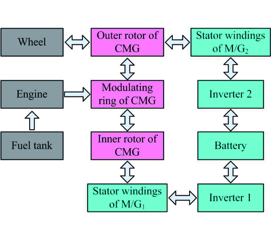
This paper proposes a new electronic-continuously variable transmission (E-CVT) system for power-split hybrid electric vehicles (HEVs). The key is to integrate two permanent magnet motor/generators (M/Gs) together with a coaxial magnetic gear (CMG). By designing the modulating ring of the CMG to be rotatable, this integrated machine can achieve both power splitting and mixing, and therefore, can seamlessly match the vehicle road load to the engine optimal operating region. With the one-side-in and one-side-out structure and the non-contact transmission of the CMG, all the drawbacks aroused by the mechanical gears and chain existing in the traditional E-CVT system can be overcome. Moreover, the proposed E-CVT system possesses the merits of small size and light weight, which are vitally important for extending the full-electric drive range of HEVs. The working principle and the design details are elaborated. By using the finite element method (FEM), the electromagnetic characteristics are analyzed.
DESIGN AND ANALYSIS OF A MAGNETIC-GEARED ELECTRONIC-CONTINUOUSLY VARIABLE TRANSMISSION SYSTEM USING FINITE ELEMENT METHOD
2010-07-29
PIER B
Vol. 24, 49-62
Analysis and Design of an UHF RFID Metal Tag Using Magnetic Composite Material as Substrate
Shih-Kang Kuo , Jen-Yung Hsu and Yung-Hsiung Hung
Using magnetic composite material as the substrate for RFID metal tag has several advantages over conventional metal tags, such as flexibility and miniaturized size. In this paper, the radiation intensity contributed by a half-wave dipole is derived based on the result of an ideal Hertzian dipole, which leads to a simple relation for thin substrate. Later on, the material constants of two materials are measured and the one capable of generating greater radiation intensity is used in the course of antenna design. A primitive pattern design demonstrates the metal tag has a satisfactory 2.7 m reading range, and a dimension of 80×22×2 mm3.
ANALYSIS AND DESIGN OF AN UHF RFID METAL TAG USING MAGNETIC COMPOSITE MATERIAL AS SUBSTRATE
2010-07-29
PIER Letters
Vol. 16, 89-97
A Compact Microstrip-Line-Fed Slot Antenna with Dual Band-Notched Characteristics for WLAN/WiMAX Applications
Fan Li , Li-Shi Ren , Gang Zhao and Yong-Chang Jiao
A compact microstrip-line-fed antenna designed by inserting two pairs of strips into a rectangular slot for achieving triple-band operation is proposed. The antenna, which occupies a small size of only 40×32×1.6 mm3, utilizes inserted strips to generate dual band-notched characteristics so that three operating bands are able to be achieved, which range from 2.2 to 2.7, 3.07 to 3.86, and 5.13 to 6.23 GHz, sufficiently covering both the 2.4/5.2/5.8 GHz WLAN and 2.5/3.5/5.5 GHz WiMAX bands. In addition, the measured results show good monopole-like radiation patterns and stable antenna gains across the three operating bands.
A COMPACT MICROSTRIP-LINE-FED SLOT ANTENNA WITH DUAL BAND-NOTCHED CHARACTERISTICS FOR WLAN/WIMAX APPLICATIONS
2010-07-29
PIER C
Vol. 15, 49-63
Novel Circular Slot UWB Antenna with Dual Band-Notched Characteristic
Guo-Ping Gao , Zhonglei Mei and Bo-Nian Li
In this paper, a novel circular slot UWB antenna with dual notched frequency band is presented and investigated. A C-shaped slot is inserted into the fed element, and a parasitic strip is printed in the circular slot, so that the proposed antenna achieves dual band-notched characteristics, respectively. The measured and simulated results show that the proposed antenna meets the requirement of wide working bandwidth of 3.1-10.6 GHz with VSWR < 2, while avoiding the interference with the 3.5 GHz WiMAX and 5.5 GHz WLAN band. Study of transfer function (amplitude of S21/group delay) and time domain characteristic (radiated pulses/power spectrum density (PSD)) correspond well with the VSWR, which indicate the dual band notched characteristic of the antenna.
NOVEL CIRCULAR SLOT UWB ANTENNA WITH DUAL BAND-NOTCHED CHARACTERISTIC
2010-07-29
PIER M
Vol. 13, 157-171
Leaky-Wave Regimes on MEMS-Loaded Transmission Lines for mm -Wave Applications
Tomas Zvolensky , Dmitry Chicherin , Antti V. Räisänen and Constantin R. Simovski
This paper presents study of controllable leaky wave modes in various planar transmission lines operating at millimetre wavelengths. Leaky wave regime is achieved by exploitation of periodic inclusions. The main goal is to obtain the scanning of the radiation angle from forward to backward direction and rather broad range of scanning angles at a given operation frequency corresponding to the mm-wave range. For this purpose we suggest to use MEMS capacitors combined with shunt strap inductors, probably grounded. This design solution allows one to significantly reduce the losses in the loaded line compared to known scanning leaky-wave antennas based on varactors or on magnetized ferrites. The design of the unit cell is done using global optimization method, and the dispersion is investigated analytically. After analytical modeling and optimization, full wave analysis is done using Ansoft HFSS v.11 environment. After the leaky wave regimes are verified, an example of a leaky-wave antenna is introduced in order to confirm possibility of beam scanning.
LEAKY-WAVE REGIMES ON MEMS-LOADED TRANSMISSION LINES FOR MM-WAVE APPLICATIONS
2010-07-29
PIER
Vol. 107, 31-46
Unique Permittivity Determination of Low-Loss Dielectric Materials from Transmission Measurements at Microwave Frequencies
Ugur Cem Hasar
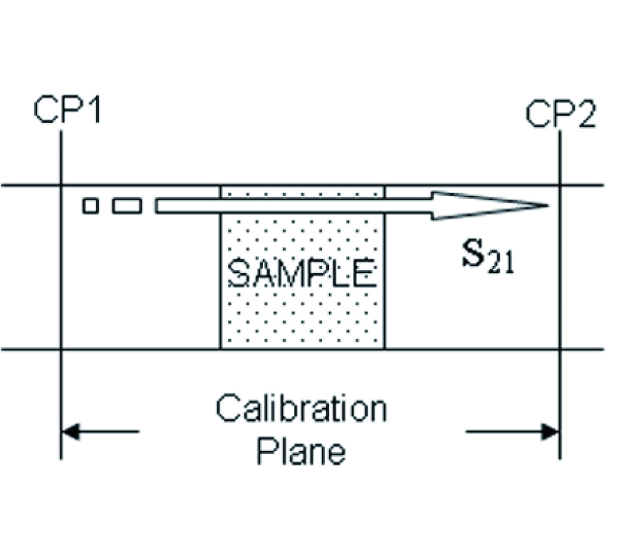
A non-resonant microwave method has been proposed for accurate complex permittivity determination of low-loss materials. The method uses two measurement data of the magnitude of transmission properties of the sample. While the first datum must correspond to a frequency point resulting in a maximum magnitude of transmission properties, the other can be any datum at a frequency different than the first datum and not far distant from the first datum. Two closed-from expressions are derived for a good initial guess using the above data. The limitations of each expression are discussed. The method has been validated by transmission measurements at X-band (8.2-12.4 GHz) of a low-loss sample located into a waveguide sample holder.
UNIQUE PERMITTIVITY DETERMINATION OF LOW-LOSS DIELECTRIC MATERIALS FROM TRANSMISSION MEASUREMENTS AT MICROWAVE FREQUENCIES