Bessel Beam Generated by the Zero-Index Metalens
Fusheng Deng,
Zhiwei Guo,
Mina Ren,
Xiaoqiang Su,
Lijuan Dong,
Yanhong Liu,
Yun Long Shi and
Hong Chen
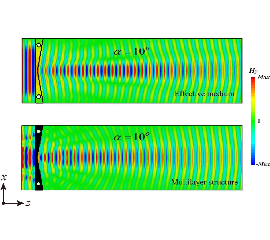
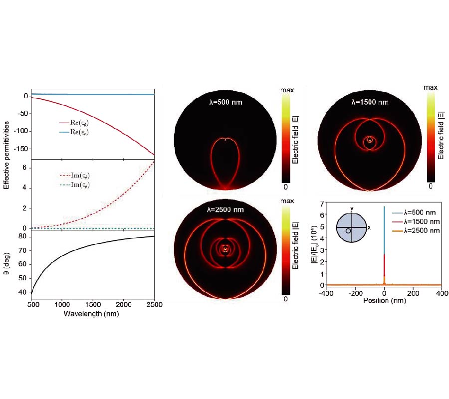
Bessel beam is an important propagation-invariant optical field. The size and shape of its central spot remain unchanged in the long-distance transmission process, which has a wide application prospect. In this paper, we find that zero-index media (ZIM) metalen can be designed to realize the unique Bessel beam. On the one hand, based on the metal-dielectric multilayered structure with sub-wavelength unit cells, the anisotropic epsilon-near-zero media (ENZ) metalen is proposed for generating the robust Bessel beam, which is immune to the defects placed in the transmission path or the inside of the structure. The ZIM metalens uncover that ENZ media provide a new way to generate Bessel beams beyond the conventional convex prisms. On the other hand, with the help of the uniform field distribution of ZIM, enhanced (multi-channel) Bessel beams based on multiple point sources (exit surfaces) are studied in the isotropic ENZ metalens. In addition, the Bessel beam generated by the ZIM metalen has also been extend to the epsilon-mu-near zero metamaterial realized by two dimensional photonic crystals. Our results not only provide a new way to generate Bessel beam based on the ZIM metalens, but also may enable their use in some optical applications, such as in fluorescence microscopy imaging, particle trapping, and wave-front tailoring.